
Introduction
Making of ALU is always a very simple task for a motivated DLD student, they only have to pour dozens of NAND gates, spoon of multiplexer, some latches as per taste and half tea spoon of Clocks, Then stir it with constant supply of electron, In the end we get our dearest ALU which talk to itself only.
However If you been into making them you would understand every bit of ALU now. You would know the internal structure and how every bit sum up to do awesome calculation for us. To understand the internal behavior of CPU, Albert Paul Malvino designed a simple model for understanding the basic functionality of Microprocessor. That design he presented is called “Simple as Possible Processor” or in short SAP.
SAP 1
Understanding these processor help the student to grab the actual logic and concept which run behind Computer to perform amazing task which can be seen in Game, Graph, Video Processing and Operating System.
Specification
- 8 bit architecture
- 16 Bytes RAM
- 8 bit W bus
- 4 bit address
- 8 bit data
- Register
- A
- B
- Output Register
- Control Unit
- 8 LEDS
SAP are so simple processor that it have only 4 bit address, which mean it can only address 16 addresses of memory that is the reason it have only 16 Bytes Ram.
Normally instruction occupies 3+ byte in modern computer and SAP instruction are maximum of size 1Byte and It memory can hold at-most 8 byte and 8 byte for data only whereas modern processor can contain trillions of instruction and can compute billions of them in a second.
SAP have only 5 instruction
| Instruction | Op Code | Description |
|---|---|---|
| LDA | 0000 | Load memory content to accumulator |
| ADD | 0001 | Add the only operand to accumulator |
| SUB | 0010 | Subtract only operand to accumulator |
| OUT | 1110 | Move accumulator data to output register |
| HLT | 1111 | HLT Stop Processing |
Example Code
LDA 8H ; Load 8H memory data to A register
ADD 9H
ADD AH
SUB BH
OUT
HLT
Only LDA, ADD, SUB have 1 operand while other don’t.Code and data is loaded to TTL (Transister-Transister Logic) before starting processor. That is the reason there is no MOV command for moving data to memory.### Instruction Format
| ADD | [16] |
| 0001 | 0010 |
| Op Code | Address |
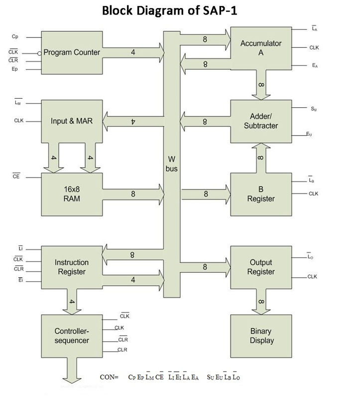
Working
Everything start from Control Unit, Control Unit turn on Counter which generate address and move it to bus then CU turn on MAR which fetch address from bus and return data at given address to the bus, then CU instruct Instruction Register (IR) to collect data from bus, Then IR move opcode to Control Sequencer (CU) and address bus to Bus. Depended on the opcode CU perform further action.
For example if instruction is LDA then CU will first resolve the address in bus to data and then instruct A register to collect it from bus. Then CU will again move to Counter to get address of another instruction for example of ADD then in this case. Then the instruction will move to IR and address to bus. According to the opcode CU first resolve address to data by consulting MAR and then move that data to B register and then move instruct ADD/SUB unit to perform appropriate work. Depending on the further instruction CU can output A register data to output LEDs
Note: Control Sequencer have 12 output to control every element of processor according to operation code.
SAP 2
SAP 2 is also in market which have 8 bit data bus and 16 bit data bus, Because of increased data bus It can address 64K of RAM. It have two more register B and TMP. SAP 2 have more instruction then SAP 1 such as JMP, SHF, MUL and etc. Detail can be seen in below table.
| SAP 1 | SAP 2 | |
|---|---|---|
| Full Form | Simple As Possible 1 | Simple as Possible 2 |
| Logical operations | Cannot be handled | Can be handled |
| Addresses | 8 bits | 16 bits |
| Opcodes | 4 bits | 8 bits |
| Instructions | Fixed length | Variable length. |
| Adder/substactor unit | Carries out simple operations like addition and subtraction | Carries out logical operations too and therefore also known as ARITHMETIC/LOGIC UNIT |
| Size of control sequencer | Smaller | Bigger due to extra registers |
| Number of instructions | Comparatively lesser | Comparatively greater |
| Register to hold the data being added or subtracted from the accumulator | B | TMP |
| Jump instructions | Not available | JM, JZ and JNZ – conditional jumpsJMP – unconditional jumps |
| Instructions | Includes instruction – LDA, ADD, SUB, OUT and HLT | Includes instructions like ADD, SUB, INR, JMP, DCR, ANA, ORA, XRA, ANI, ORI, XRI, etc. |
| Display to show outputs in the LEDs | Binary | Hexadecimal |